- 您现在的位置:买卖IC网 > Sheet目录1902 > AT32UC3C2512C-A2UT (Atmel)IC MCU AVR32 512K FLASH 64TQFP
60
32117DS–AVR-01/12
AT32UC3C
7.7
Flash Characteristics
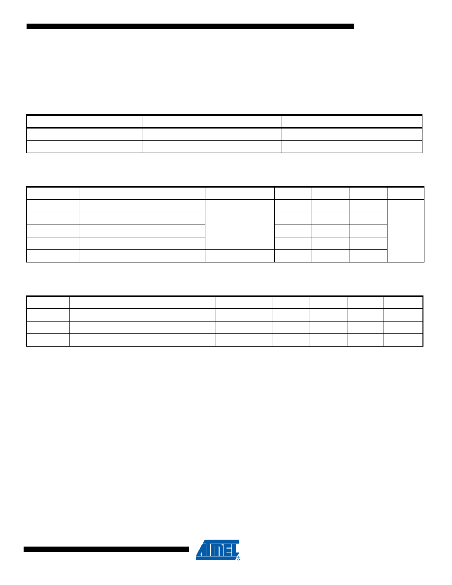
Table 7-15 gives the device maximum operating frequency depending on the number of flash
wait states. The FSW bit in the FLASHC FSR register controls the number of wait states used
when accessing the flash memory.
Table 7-15.
Maximum Operating Frequency
Flash Wait States
Read Mode
Maximum Operating Frequency
0
1 cycle
33MHz
1
2 cycles
66MHz
Table 7-16.
Flash Characteristics
Symbol
Parameter
Conditions
Min
Typ
Max
Unit
tFPP
Page programming time
fCLK_HSB = 66MHz
4.3
ms
t
FPE
Page erase time
4.3
tFFP
Fuse programming time
0.6
tFEA
Full chip erase time (EA)
4.9
t
FCE
JTAG chip erase time (CHIP_ERASE)
f
CLK_HSB = 115 kHz
640
Table 7-17.
Flash Endurance and Data Retention
Symbol
Parameter
Conditions
Min
Typ
Max
Unit
NFARRAY
Array endurance (write/page)
100k
cycles
N
FFUSE
General Purpose fuses endurance (write/bit)
1k
cycles
t
RET
Data retention
15
years
发布紧急采购,3分钟左右您将得到回复。
相关PDF资料
AT32UC3C2512C-A2ZT
IC MCU 32BIT 512KB FLASH 64TQFP
AT32UC3L016-D3HR
MCU AVR32 16K FLASH 48TTLGA
AT42QT5480-CU QS444
IC SENSOR DUAL TOUCH 49-BGA
AT6010H-4QI
IC FPGA 4NS 240PQFP
AT80C31X2-SLRUM
MCU ROMLESS 31X2 5V 44-PLCC
AT80C51RD2-SLRUM
IC MCU 80C51 HI PERFORM 44PLCC
AT85C51SND3B1-RTTUL
IC DECODER/ENCODER DGTL 100-LQFP
AT87251G2D-RLTUM
IC MCU 8/16BIT 32K OTP 44-VQFP
相关代理商/技术参数
AT32UC3C2512C-A2ZR
功能描述:32位微控制器 - MCU 512KB FL,-40/125oC AUTO
RoHS:否 制造商:Texas Instruments 核心:C28x 处理器系列:TMS320F28x 数据总线宽度:32 bit 最大时钟频率:90 MHz 程序存储器大小:64 KB 数据 RAM 大小:26 KB 片上 ADC:Yes 工作电源电压:2.97 V to 3.63 V 工作温度范围:- 40 C to + 105 C 封装 / 箱体:LQFP-80 安装风格:SMD/SMT
AT32UC3C2512C-A2ZT
功能描述:32位微控制器 - MCU 512KB FL,-40/125oC AUTO
RoHS:否 制造商:Texas Instruments 核心:C28x 处理器系列:TMS320F28x 数据总线宽度:32 bit 最大时钟频率:90 MHz 程序存储器大小:64 KB 数据 RAM 大小:26 KB 片上 ADC:Yes 工作电源电压:2.97 V to 3.63 V 工作温度范围:- 40 C to + 105 C 封装 / 箱体:LQFP-80 安装风格:SMD/SMT
AT32UC3C2512C-Z2UR
制造商:Atmel Corporation 功能描述:MCU 32-bit AT32 AVR RISC 512KB Flash 3.3V/5V 64-Pin QFN EP T/R 制造商:Atmel Corporation 功能描述:512KB FLASH 64QFN(-40?C TO 85?C) T&R - Tape and Reel 制造商:Atmel Corporation 功能描述:IC MCU 32BIT 512KB FLASH 64QFN 制造商:Atmel Corporation 功能描述:32-bit Microcontrollers - MCU 512KB Flash 64QFN (-40oC to 85oC) 制造商:Atmel Corporation 功能描述:512KB Flash 64QFN(-40C to 85C) T&R
AT32UC3C2512C-Z2UT
制造商:Atmel Corporation 功能描述:512KFLASH AUTO - Trays
AT32UC3C2512C-Z2ZES
制造商:Atmel Corporation 功能描述:512KFLASH UC3C AUTO - QFN64 ENG SAMPLE - Bulk
AT32UC3C2512C-Z2ZR
功能描述:32位微控制器 - MCU 512KB FL,-40/125oC AUTO
RoHS:否 制造商:Texas Instruments 核心:C28x 处理器系列:TMS320F28x 数据总线宽度:32 bit 最大时钟频率:90 MHz 程序存储器大小:64 KB 数据 RAM 大小:26 KB 片上 ADC:Yes 工作电源电压:2.97 V to 3.63 V 工作温度范围:- 40 C to + 105 C 封装 / 箱体:LQFP-80 安装风格:SMD/SMT
AT32UC3C2512C-Z2ZT
功能描述:32位微控制器 - MCU 512KB FL,-40/125oC AUTO
RoHS:否 制造商:Texas Instruments 核心:C28x 处理器系列:TMS320F28x 数据总线宽度:32 bit 最大时钟频率:90 MHz 程序存储器大小:64 KB 数据 RAM 大小:26 KB 片上 ADC:Yes 工作电源电压:2.97 V to 3.63 V 工作温度范围:- 40 C to + 105 C 封装 / 箱体:LQFP-80 安装风格:SMD/SMT
AT32UC3C264C-A2UR
功能描述:32位微控制器 - MCU UC3C 64K FLASH 16K SRAM
RoHS:否 制造商:Texas Instruments 核心:C28x 处理器系列:TMS320F28x 数据总线宽度:32 bit 最大时钟频率:90 MHz 程序存储器大小:64 KB 数据 RAM 大小:26 KB 片上 ADC:Yes 工作电源电压:2.97 V to 3.63 V 工作温度范围:- 40 C to + 105 C 封装 / 箱体:LQFP-80 安装风格:SMD/SMT